How the J113 N-Channel Transistor Works in Electronic Circuits
The J113 is a versatile N-channel field-effect transistor that’s widely used in circuits needing reliable switching and signal amplification. In this article, you’ll learn about its features, benefits, and practical applications.Catalog
Overview of J113
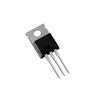
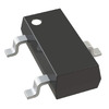
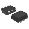
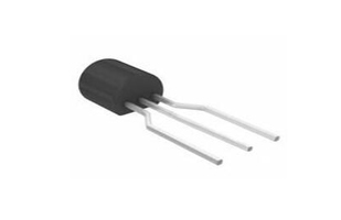
The J113 is part of the J11x series of N-channel field-effect transistors, designed with TO-92 and SOT-23 packaging. It shares its family line with similar transistors like the J111 and J112. This transistor is versatile, primarily used in applications such as choppers, sample-and-hold circuits, current limiters, and various switching setups. Its performance in analog circuits makes it a go-to choice for tasks that require smooth and reliable switching and current management. With a structure that enables easy integration into compact circuits, the J113 offers the practical flexibility needed in both industrial and consumer applications.
J113 Pin Configuration
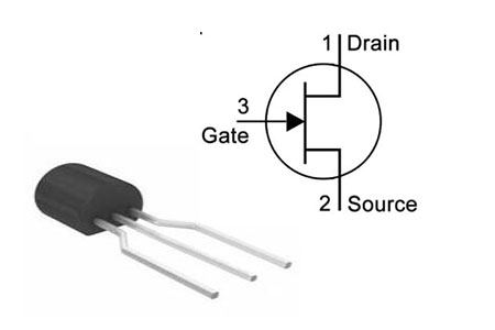
J113 CAD Model
J113 Symbol
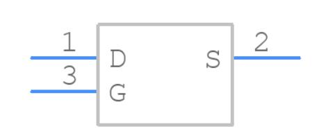
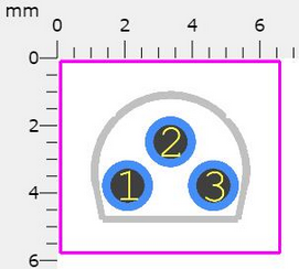
J113 Footprint
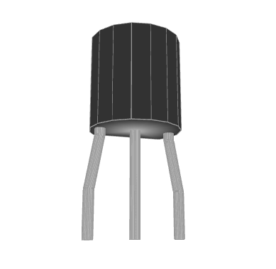
J113 3D Model
J113 Specifications
Technical specifications, features, characteristics, and components with comparable specifications of ON Semiconductor J113.
[TABLE OF J113 Specifications]
J113 Features
Package Options
The J113 is available in two convenient package types, TO-92 and SOT-23, allowing you to choose the format that best suits your project requirements. This flexibility makes it easier to fit into various circuit designs and layouts.
N-Channel JFET Transistor
This N-channel JFET (junction field-effect transistor) has a symmetrical design, making it suitable for a wide range of switching and amplification applications. Its design promotes efficient performance in both digital and analog circuits.
Maximum Drain to Gate Voltage
The J113 can handle a maximum drain-to-gate voltage of 35V, making it robust for many applications that require stable performance under higher voltage levels.
Reverse Gate to Source Voltage
With a maximum reverse gate-to-source voltage of -35V, the J113 is built to withstand reverse voltages, which helps protect it from potential reverse polarity damage.
Continuous Gate Current
The J113 supports a continuous gate current of up to 50mA, enabling it to manage moderate current loads effectively. This capability makes it versatile across various switching and amplifying uses.
Gate to Source Cutoff Voltage
The gate-to-source cutoff voltage ranges between -5V and -3V, allowing the J113 to maintain control over the current flow, providing effective switching capabilities for different applications.
Maximum Power Dissipation
With a power dissipation rating of 625mW, the J113 can handle a fair amount of power without overheating, ensuring reliability in continuous operation.
Temperature Range
The J113 is rated for storage and operation in a temperature range of -55°C to +150°C, making it suitable for environments with extreme temperature variations.
Interchangeable Drain and Source
One of the unique features of the J113 is that its drain and source terminals are interchangeable, giving you added flexibility in designing circuits and making it easier to integrate into various setups.
Benefits of Using J113
High Switching Speed
One benefit of using the J113 is its high switching speed, making it an effective choice when you need quick transitions in electronic circuits. This feature helps improve overall circuit responsiveness, especially in applications requiring frequent switching.
Reliable Frequency Response
The J113 has a dependable response to different frequencies, ensuring consistent performance across a range of operations. This benefit makes it a strong choice for audio amplifiers and other frequency-sensitive applications, where stability and accuracy are valued.
Accurate Signal Processing
The J113 enhances the accuracy of signal processing, making it a dependable option for circuits that need clear and precise signal amplification. With this transistor, you’re more likely to achieve high-quality output, especially in low-level signal amplification applications.
Cost-Effective Solution
The J113 offers a cost-effective option for many projects, allowing you to incorporate reliable components without driving up costs. This benefit is ideal for both individual projects and larger-scale manufacturing where keeping costs down is valuable.
Minimal Insertion Loss
Insertion loss is kept to a minimum with the J113, ensuring that signals remain strong throughout the circuit. This low-loss feature helps maintain signal integrity, an advantage in both audio and analog switching applications.
J113 Applications
Audio Preamplifiers
The J113 is frequently used in audio preamplifiers to boost low-level audio signals. This application helps achieve a stronger output, making the audio signal more robust for further amplification or processing.
High Gain Amplifiers
In high gain amplifiers, the J113 works effectively to strengthen the input signal. It’s ideal for applications where you need a significant increase in signal strength without sacrificing clarity.
Sensor and Detector Circuits
You’ll find the J113 in various sensor and detector circuits, where it enhances the sensitivity and accuracy of these devices. It works well to stabilize signals from sensors, which is useful in many measurement and control systems.
Current Limiting Circuits
The J113 serves as a valuable component in current limiting circuits, protecting other components by controlling the current flow. This application is especially useful in preventing circuit overloads and ensuring steady operation.
Analog Switching Circuits
The J113 performs reliably in analog switching circuits, allowing for seamless transitions between different analog signals. This feature is particularly valuable in signal processing, where smooth switching is often required.
Low-Level Signal Amplification
The J113 is well-suited for low-level signal amplification, helping to enhance weak signals while maintaining a clear output. It’s a practical choice when you need to amplify small signals in both audio and other signal processing applications.
Usage Guidelines for J113
The J113 transistor serves well in various electronic applications, especially where controlled current flow or precise switching is required. You’ll often find it enhancing circuit performance in areas like current limiting, chopper applications, and analog switching circuits. In high-gain amplifiers, the J113 works to strengthen electronic signals, ensuring that signals remain stable and clear. Whether it's applied in an industrial setup or a personal electronics project, the J113 offers reliability and performance, making it a valuable component in both basic and complex electronic designs.
Equivalents of J113
[TABLE OF J113 Equivalent]
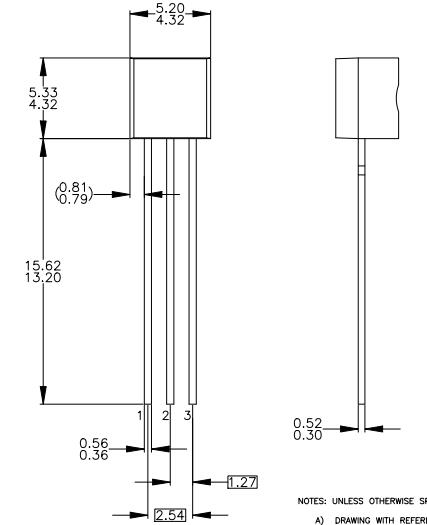
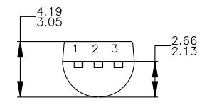
J113 Dimension Outline
Manufacturer Information for J113
ON Semiconductor, now known as onsemi, is the manufacturer behind the J113. This American semiconductor supplier was part of the Fortune 500 before moving into the Fortune 1000 in 2020. Their product line spans power and signal management, logic, discrete components, and custom devices used across a wide range of fields, including automotive, communications, computing, consumer products, and LED lighting. They also cater to sectors like medical technology, military, aerospace, and power applications, offering reliable and high-quality semiconductor solutions for varied technological needs
За нас
ALLELCO LIMITED
Прочетете още
Бързо запитване
Моля, изпратете запитване, ние ще отговорим незабавно.
често задавани въпроси [FAQ]
1. What are the main uses of the J113 transistor?
The J113 transistor is often used for low-level analog switching, sample-and-hold circuits, and chopper-stabilized amplifiers. Its design makes it suitable for controlling smaller signals with precision, which is helpful in various signal processing applications where smooth switching is needed.
2. What is the maximum voltage rating for the J113?
The J113 can handle a maximum DC supply voltage of 30V. This allows it to perform well in circuits with moderate voltage demands without risking breakdown or damage.
3. What is the operating temperature range of the J113?
The J113 operates reliably within a temperature range of -55°C to +150°C. This wide range makes it suitable for use in both high-temperature and low-temperature environments, adding to its flexibility in different applications.
4. How does a JFET like the J113 function?
A JFET, or junction field-effect transistor, controls current by using an electric field to manage the flow through its conducting channel. In the J113, the gate controls the current between the source and drain, offering high input impedance and low noise, which makes it ideal for sensitive applications that need clear signal amplification.
Complete Guide to the 2N3906 PNP Transistor
на 2024/11/14
Всичко за IRF530 MOSFET
на 2024/11/14
Популярни публикации
-
Какво е GND във веригата?
на 1970/01/1 3191
-

Ръководство за конектор RJ-45: RJ-45 Connector Color кодове, схеми за окабеляване, R-J45 приложения, RJ-45 таблици с данни
на 1970/01/1 2760
-
Разбиране на напреженията за захранване в Electronics VCC, VDD, VEE, VSS и GND
на 0400/11/18 2452
-
Видове конектори за влакна: SC срещу LC и LC срещу MTP
на 1970/01/1 2222
-

Сравнение между DB9 и RS232
на 1970/01/1 1846
-
Какво е батерия LR44?
Електричеството, тази повсеместна сила, тихо прониква във всеки аспект от ежедневието ни, от тривиални джаджи до животозастрашаващо медицинско оборудване, тя играе мълчалива роля.Въпреки това, наистина схващането на ...на 1970/01/1 1818
-
Разбиране на основите: Съпротива на индуктивността и заден план
В сложния танц на електротехниката трио от основни елементи заема централна сцена: индуктивност, съпротива и капацитет.Всеки носи уникални черти, които диктуват динамичните ритми на електронните вериги.Тук ние тръгва...на 1970/01/1 1772
-

CR2430 Изчерпателно ръководство за батерията: Спецификации, приложения и сравнение с CR2032 батерии
Какво е CR2430 батерия?Предимства на батериите CR2430НормаCR2430 Приложения на батериятаCR2430 еквивалентCR2430 срещу CR2032Размер на батерията CR2430Какво да търсите, когато купувате CR2430 и еквивалентитеЛист с данни PDFЧесто задавани въп...на 1970/01/1 1747
-
Какво е RF и защо го използваме?
Технологията на радиочестотната (RF) е ключова част от съвременната безжична комуникация, което позволява предаване на данни на дълги разстояния без физически връзки.Тази статия се задълбочава в основите на RF, обяснява...на 1970/01/1 1734
-
Изчерпателно ръководство за HFE в транзисторите
Транзисторите са решаващи компоненти в съвременните електронни устройства, което позволява усилване и управление на сигнала.Тази статия се задълбочава в знанията около HFE, включително как да изберете стойността на HFE ...на 5600/11/18 1720
